
High-Density Parchment Paper Papertronics with Laser-Carved Hydrophilic Channels
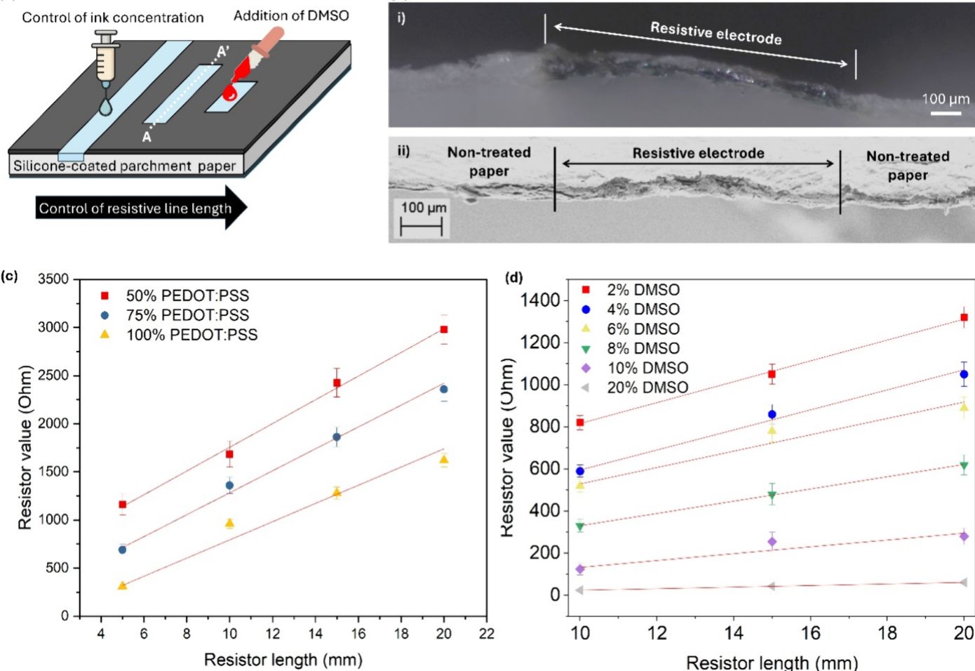
Researchers developed a method to create high-resolution papertronics using hydrophobic parchment paper and a laser to carve hydrophilic channels. The technique allows for precise printing of conductive traces and functional components like resistors and capacitors, achieving better resolution than previous wax-based methods. The circuits, made with materials like PEDOT:PSS and PVA gel, were tested for durability and showed resistance to degradation in soil, with options for encapsulation to enhance longevity. This advancement offers a low-cost, flexible, and environmentally friendly approach to electronic circuit fabrication.
Scientists used laser-carved parchment paper to create flexible electronic circuits with high resolution and recyclable materials.
This method offers a low-cost, eco-friendly alternative for making paper-based electronics that could be used in disposable or biodegradable devices.
The innovation supports sustainable technology development by combining traditional materials with modern fabrication techniques for practical, real-world applications.
upbeatBytes summarizes in its own words and links to the original publisher — it doesn't host the article.